- 您现在的位置:买卖IC网 > Sheet目录1997 > ICS843001AG-21LFT (IDT, Integrated Device Technology Inc)IC SYNTHESIZER LVPECL 24-TSSOP
ICS843001-21
FEMTOCLOCKS CRYSTAL-TO-3.3V LVPECL FREQUENCY SYNTHESIZER
IDT / ICS LVPECL FREQUENCY SYNTHESIZER
2
ICS843001AG-21 REV. AMARCH 15, 2007
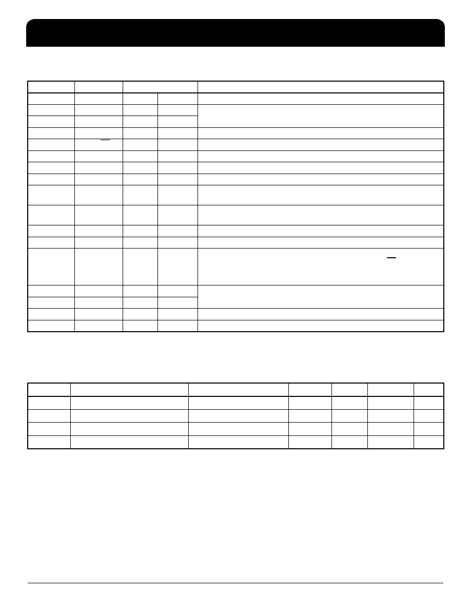
Table 1. Pin Descriptions
NOTE: Pullup and Pulldown refer to intenal input resistors. See Table 2, Pin Characteristics, for typical values.
Table 2. Pin Characteristics
Number
Name
Type
Description
1VCCO_CMOS
Power
Output supply pin for REF_CLK output.
2, 3
N0, N1
Input
Pullup
Output divider select pins. Default ÷4. LVCMOS/LVTTL interface levels.
See Table 3C.
4
N2
Input
Pulldown
5VCCO_PECL
Power
Output supply pin for LVPECL output.
6, 7
Q0, Q0
Output
Differential output pair. LVPECL interface levels.
8, 23
VEE
Power
Negative supply pins.
9VCCA
Power
Analog supply pin.
10
VCC
Power
Core supply pin.
11,
12
XTAL_OUT1,
XTAL_IN1
Input
Parallel resonant crystal interface.
XTAL_OUT1 is the output, XTAL_IN1 is the input.
13,
14
XTAL_OUT0,
XTAL_IN0
Input
Parallel resonant crystal interface.
XTAL_OUT0 is the output, XTAL_IN0 is the input.
15
TEST_CLK
Input
Pulldown
LVCMOS/LVTTL clock input.
16, 17
SEL0, SEL1
Input
Pulldownp
Input MUX select pins. LVCMOS/LVTTL interface levels. See Table 3D.
18
MR
Input
Pulldown
Active HIGH Master Reset. When logic HIGH, the internal dividers are reset
causing the true output Q0 to go low and the inverted output Q0 to go high.
When logic LOW, the internal dividers and the outputs are enabled.
LVCMOS/LVTTL interface levels.
19, 20
M0, M1
Input
Pulldown
Feedback divider select pins. Default ÷32. See Table 3B
LVCMOS/LVTTL interface levels.
21
M2
Input
Pullup
22
OE_REF
Input
Pulldown
Reference clock output enable. Default Low. LVCMOS/LVTTL interface levels.
24
REF_CLK
Output
Reference clock output. LVCMOS/LVTTL interface levels.
Symbol
Parameter
Test Conditions
Minimum
Typical
Maximum
Units
CIN
Input Capacitance
4
pF
RPULLUP
Input Pullup Resistor
51
k
RPULLDOWN Input Pulldown Resistor
51
k
ROUT
Output Impedance
7
发布紧急采购,3分钟左右您将得到回复。
相关PDF资料
ICS843001AGI-22LFT
IC SYNTHESIZER LVPECL 24-TSSOP
ICS843001AKI-40LF
IC SYNTHESIZER LVPECL 16-VFQFPN
ICS843002AGI-01LF
IC SYNTHESIZER LVPECL 20-TSSOP
ICS843002AKI-41LF
IC SYNTHESIZER LVPECL 32-VFQFPN
ICS843004AG-02LF
IC SYNTHESIZER LVPECL 24-TSSOP
ICS843004AGI-04LF
IC SYNTHESIZER LVPECL 24-TSSOP
ICS843021AGLFT
IC CLK GENERATOR LVPECL 8-TSSOP
ICS843022AGLF
IC CLK GENERATOR LVPECL 8-TSSOP
相关代理商/技术参数
ICS843001AG-21T
制造商:ICS 制造商全称:ICS 功能描述:FEMTOCLOCKS⑩ CRYSTAL-TO-3.3V LVPECL FREQUENCY SYNTHESIZER
ICS843001AGI-22
制造商:ICS 制造商全称:ICS 功能描述:FEMTOCLOCKS? CRYSTAL/LVCMOS-TO-3.3V, 2.5V LVPECL FREQUENCY SYNTHESIZER
ICS843001AGI-22LF
功能描述:IC SYNTHESIZER LVPECL 24-TSSOP RoHS:是 类别:集成电路 (IC) >> 时钟/计时 - 时钟发生器,PLL,频率合成器 系列:HiPerClockS™, FemtoClock™ 标准包装:1,000 系列:Precision Edge® 类型:时钟/频率合成器 PLL:无 输入:CML,PECL 输出:CML 电路数:1 比率 - 输入:输出:2:1 差分 - 输入:输出:是/是 频率 - 最大:10.7GHz 除法器/乘法器:无/无 电源电压:2.375 V ~ 3.6 V 工作温度:-40°C ~ 85°C 安装类型:表面贴装 封装/外壳:16-VFQFN 裸露焊盘,16-MLF? 供应商设备封装:16-MLF?(3x3) 包装:带卷 (TR) 其它名称:SY58052UMGTRSY58052UMGTR-ND
ICS843001AGI-22LFT
功能描述:IC SYNTHESIZER LVPECL 24-TSSOP RoHS:是 类别:集成电路 (IC) >> 时钟/计时 - 时钟发生器,PLL,频率合成器 系列:HiPerClockS™, FemtoClock™ 标准包装:27 系列:Precision Edge® 类型:频率合成器 PLL:是 输入:PECL,晶体 输出:PECL 电路数:1 比率 - 输入:输出:1:1 差分 - 输入:输出:无/是 频率 - 最大:800MHz 除法器/乘法器:是/无 电源电压:3.135 V ~ 5.25 V 工作温度:0°C ~ 85°C 安装类型:表面贴装 封装/外壳:28-SOIC(0.295",7.50mm 宽) 供应商设备封装:28-SOIC 包装:管件
ICS843001AGI-22T
制造商:ICS 制造商全称:ICS 功能描述:FEMTOCLOCKS? CRYSTAL/LVCMOS-TO-3.3V, 2.5V LVPECL FREQUENCY SYNTHESIZER
ICS843001AGI-23
制造商:ICS 制造商全称:ICS 功能描述:FEMTOCLOCKS⑩ CRYSTAL-TO-3.3V LVPECL/LVCMOS FREQUENCY SYNTHESIZER
ICS843001AGI-23LF
功能描述:IC SYNTHESIZER LVPECL 24-TSSOP RoHS:是 类别:集成电路 (IC) >> 时钟/计时 - 时钟发生器,PLL,频率合成器 系列:HiPerClockS™, FemtoClock™ 标准包装:27 系列:Precision Edge® 类型:频率合成器 PLL:是 输入:PECL,晶体 输出:PECL 电路数:1 比率 - 输入:输出:1:1 差分 - 输入:输出:无/是 频率 - 最大:800MHz 除法器/乘法器:是/无 电源电压:3.135 V ~ 5.25 V 工作温度:0°C ~ 85°C 安装类型:表面贴装 封装/外壳:28-SOIC(0.295",7.50mm 宽) 供应商设备封装:28-SOIC 包装:管件
ICS843001AGI-23LFT
功能描述:IC SYNTHESIZER LVPECL 24-TSSOP RoHS:是 类别:集成电路 (IC) >> 时钟/计时 - 时钟发生器,PLL,频率合成器 系列:HiPerClockS™, FemtoClock™ 标准包装:27 系列:Precision Edge® 类型:频率合成器 PLL:是 输入:PECL,晶体 输出:PECL 电路数:1 比率 - 输入:输出:1:1 差分 - 输入:输出:无/是 频率 - 最大:800MHz 除法器/乘法器:是/无 电源电压:3.135 V ~ 5.25 V 工作温度:0°C ~ 85°C 安装类型:表面贴装 封装/外壳:28-SOIC(0.295",7.50mm 宽) 供应商设备封装:28-SOIC 包装:管件